Tag: Teardown

  • Teardown of 5K Retina Dispay iMac Reveals What’s Inside

    Teardown of 5K Retina Dispay iMac Reveals What’s Inside

    Continuing with its fascination for Apple products, iFixit, who are known for surgically removing all the organs of devices and laying them side by side, has acquired and disassembled the new iMac with 5K Retina display.

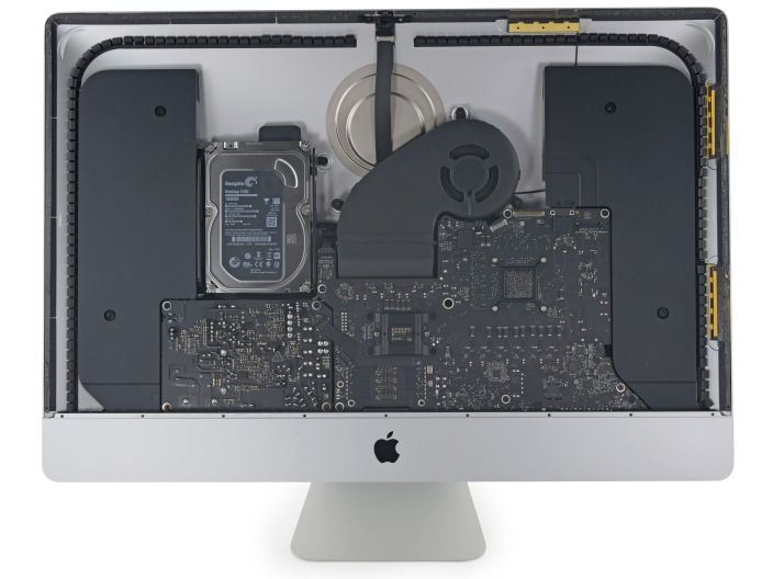
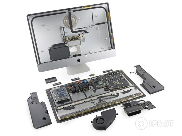
    Apple’s newest iMac continues to use many of the same design elements from previous iMacs, including an easily accessible RAM upgrade slot,  the same SSD, and logic board on the back of the device. With the RAM slot, users will be able to install their own RAM modules with little trouble.

    retinateardowna

    Along with an AMD Radeon M290X GPU and i5-4690 processor from Intel, the iMac contains SK Hynix 256 MB GDDR5 SGRAM. It uses the same SanDisk PCIe SSD as the late 2013 Retina MacBook Pro, with Marvell Controller, and it uses the same AirPort/Bluetooth card that was used in the 2013 27-inch iMac.

    Though, the processor, GPU, and display controller (sporting a wider display data cable) have received significant upgrades. The teardown also revealed that the 5K display, which sports the screen resolution of 5120 x 2880, has been manufactured by LG Display. It is the same supply partner that has also manufactured previous generation iMac displays.

    retinateardown1

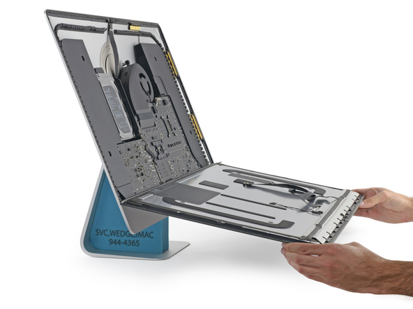
    The 27-inch iMac with Retina 5K display earned a repairability score of 5 out of 10, the same score earned by the 2013 27-inch iMac. iFixit pointed out that the RAM, hard drive, and CPU are user replaceable with some adhesive cutting, but removing the glass and LCD panel from the machine remains a difficult task.


  • Teardown of the iPhone 6 and 6 Plus Reveals What’s Inside

    Teardown of the iPhone 6 and 6 Plus Reveals What’s Inside

    Apple’s flagship is now available for anyone who has got the money for it. The phone got polarising reviews with Apple fans sticking by their device and Android fans turning social media against the new iPhones using tons of memes. As always, it is now time to rip apart and unveil all the secret sauces that went into making the new jewel in Apple’s crown. The tear down of both phones showed us that they are pretty interesting on the inside.

    First up, the iPhone 6 with a 4.7 inch display. A Japanese blog called ‘Mac Otakara’ disassembled the phone. They found that the 1810 mAh battery on the device was fastened to the chassis with adhesive tabs. The phone has received some internal tweaks to adapt to the slimmer design. It has a linear oscillating type vibrating motor that sits on the right with the battery. The phone is said to have 1GB RAM.

    The
    The Phones were torn down by IFixit and Mac Otakara

    The iPhone 6 Plus, on the other hand, was unraveled by iFixit who are known for surgically removing all the organs of devices and laying them side by side. The battery on Apple’s biggest iPhone yet stands at 2915 mAh. The battery is bigger in comparison to Samsung’s S5 (2800mAh) which was released earlier this year. Like the Samsung flagship, the iPhone 6 Plus has a full HD(1920X1080) display.

    iFixit confirmed that the device holds an Elpida 1 GB LPDDR3 RAM. It is an entire gigabyte less than Samsung’s S5 and 2 gigabyte less than the Note 4. The company also confirmed that the smaller sibling, iPhone 6 also carries the same amount of RAM. The devices are powered by Apple’s A8 chipset.

    The Camera Module with OIS is beautiful to look at.
    The Camera Module with OIS is beautiful to look at.

    The camera modules on the phones were impressive to see. This new cameras has optical image stabilization, and it sure looks beautiful on the inside.

    The 128GB NAND flash memory has been supplied by SK Hynix. Other features that were found inside include the Wi-Fi module supplied by Murata, touch screen controller by Broadcom, power amplifier module by TriQuint and gyroscope and accelerometer combo supplied by InvenSense.

    Apple has claimed that the new devices have better battery life and are faster than the previous generations. Considering its higher end phones have the same amount of RAM as there is in the Moto E, it will be interesting to see how the phones handle the new additions such as the much-touted interconnectivity features.

  • About Time! Google Glass Cracked Open In Teardown

    About Time! Google Glass Cracked Open In Teardown

    It was bound to happen at some point, and condolences to whomever sacrificed their frames for the greater good aside, we’ve got our first look at the components from Google Glass and how they’re fitted together.

    The internet owes a deep thanks to Scott Torborg and Star Simpson who did a detailed tear-down post on the Google Glass.

    Some of the motivation for the tear down was purely technological while some of it was driven by the growing concerns about privacy and personal security in the US.

    “Growing up on a rich diet of dystopian tech fiction, we were filled with both intrigue and concern about Glass and decided to take our model apart to bring you a detailed view into the electronics guts of the device.

    It is not surprising that the camera is similar in quality and resolution to cameras found in your everyday smartphone:

    “The Glass camera seems to be of typical smartphone-level size and format. It is not coaxially aligned with the wearer’s eye. The camera and display appear to talk to the CPU independently, with no direct connection between each other.

    The main board, which is held in place with “lots of paste.” Removing said paste revealed a TI OMAP4430 chip and a 16GB SanDisk flash chip. Next was the battery, which also required tearing the plastic in order to get to it. Obviously, this means users cannot replace the battery on their own. The rest of the teardown is detailed in extensive pictures, which you can check out at the link at the bottom.

    Google Glass

    According to the Google Glass Tech specs page, Glass has a 5-megapixel camera that can shoot video in 720p. It supports 802.11 b/g Wi-Fi and Bluetooth. Audio is provided by a bone conduction transducer, and the display is “the equivalent of a 25-inch high definition screen from eight feet away.” As for buttons and connectors, Glass has a Listen button, on/off button, capture button, touch sensitive area, and Micro USB port for charging. There’s also a status LED and rear-facing sensor array.

    [Catwig]

  • HTC One Gets iFixit Teardown, Reveals Low Repairability, High Durability

    HTC One Gets iFixit Teardown, Reveals Low Repairability, High Durability

    The HTC One looks like bulletproof phone, with a hefty aluminium – glass body and no removable back. 

    However, there is a price to pay for its robust unibody design. Teardown specialists iFixit found that the new phone is practically impossible to open up and repair. It got a score of one, one out of ten that is.

     htc one

    With the release of the HTC One, the manufacturer has bet a whole lot on the hardware as a proving point in their history. With this release, the company known as HTC says that they’ve done the best they’re able at the moment – this is the HTC One, and it’s named that for a reason. According to iFixit, this device is just about the most difficult smartphone to tear apart they’ve come across.

    The process took 19 steps and ended with the handset being give a score of one (out of ten) in terms or repairability. Of course, these days we don’t see many people repairing their smartphones, but instead buying new. In that respect, a score of one flips nicely to mean that the One is a solid device. In fact, the teardown noted that the “solid external construction improves durability.”

    htc one

    The issues at hand? iFixit said it’s nearly impossible to open the One without damaging the back cover. Again, go figure, it’s a unibody phone. The battery is also stuck under the motherboard and is not replaceable and there’s a lot of copper shielding that causes issues while trying to remove parts. The screen can’t be replaced without removing the back cover, though, so you’ll want to make sure you don’t drop your One all over the floor.

    [iFixit]

  • Video : Sony Xperia Tablet Z Teardown

    Video : Sony Xperia Tablet Z Teardown

    The Sony Xperia Tablet Z is currently the thinnest tablet yet at only 6.9mm and it weighs just 495grams. That’s actually thinner than the 7.9mm Xperia Z. To find out how its top notching hardware gets packed in such a slim profile, Sony has released its official tear down of the Xperia Tablet Z. Of course, dissecting the tablet would automatically void its warranty, so don’t try this at home (if you have one, that is, which is highly unlikely for people living in India)!

    sony xperia tablet z

    The Sony Xperia Tablet Z was announced back in January, and has gone on sale in Japan today, it will also launch in the US and Europe shortly followed by Asia, the device comes with Android 4.1 Jelly Bean and it features a 10.1 inch full HD display with a resolution of 1920 x 1080 pixels.

    Other specifications on the Sony Xperia Tablet Z include a quad core Qualcomm APQ8064 processor clocked at 1.5GHz, plus 2GB of RAM and 32GB of built in storage, and there is also a rear facing 8.1 megapixel camera with Sony’s Exmor R sensor.

    The Sony Xperia Tablet Z teardown begins with cracking the device open. Sounds easy? Well, think again. Since the tablet is resistant to dust and water damage, it comes as no surprise that taking its back cover off isn’t a job for everyone. Once that’s unglued, the delicate part dismantling process begins, starting with the Sony-made lithium-ion battery weighing 130 grams and then moving on to the smaller components. There’s plenty of glue and tape holding the Xperia Tablet Z together, which leads us to believe that its repairability score might not be very high.

    [Via Sony Blog]

  • Google’s Nexus 7 Gets the iFixit Treatment – Teardown

    Google’s Nexus 7 Gets the iFixit Treatment – Teardown

    Google’s Nexus 7 Tab joins the iFixit list of tear downs, with the tablet being torn apart by the experts. Several discoveries were made during the teardown, including the fact that the display is permanently attached to the gorilla glass front. The 7-inch, 1280×800 HD display is manufactured by Hydis and designated model HV070WX2.

    for parts 

    •  Kingston KE44B-26BN/8GB 8GB flash
       
    •  Realtek ALC5642
       
    •  ELAN eKTF36248WS
       
    •  ELAN eKTH10368WS
       
    •  Texas Instruments 22C96ST SN75LVDS83B (www.ti.com/product/sn75lvds83b)
       
    •  TI20 MI60
       
    • Hynix HTC2G83CFR DDR3 RAM


    Motherboard Parts:

     
    •  NVIDIA T30L Tegra 3 processor
       
    •  Hynix HTC2G83CFR DDR3 RAM
       
    •  Max 77612A inverting switching regulator
       
    •  AzureWave AW-NH665 wireless module
       
    •  Broadcom BCM4751 integrated monolithic GPS receiver
       
    •  NXP 65N04
       
    •  Invensense MPU-6050 gyro and accelerometer
       
     
    We Are soon going Hands on with the Nexus 7 , Stay Tuned
  • Bam and its torn down! The iPhone 4s Gets the iFixit !

    Bam and its torn down! The iPhone 4s Gets the iFixit !

    The folks over at iFixit cant refrain from their antic and this time around they ripped the Jesus phone before it reached out to people. They have a humorously documented rip down of the new “Siri” laden smartphone. A looksie i promise will bring a smile to your face follow the link below!

    The findings are not too shocking with the same 512MB of Ram Courtesy Samsung/Elpida (both DDR2), and the following chips:

    • Qualcomm RTR8605 Multi-band/mode RF Transceiver.

    • Skyworks 77464-20 Load-Insensitive Power Amplifier (LIPA®) module developed for WCDMA applications)

    • Avago ACPM-7181 Power Amplifier

    • TriQuint TQM9M9030 Multi-Mode Quad-Band Power Amplifier Module.

    • TriQuint TQM66052 (possibly a PA-Duplexer Module)

    • Qualcomm MDM6610 chipset (an upgrade from the iPhone 4’s MDM6600)

    • Apple 338S0973, newer version of the Cirrus Logic audio codec found in the original iPhone 4

    •  “PM8028,” which is a Qualcomm power management IC.


    iFixit

  • Xiaomi phone gets the take apart treatment

    Xiaomi phone gets the take apart treatment

    The highly talked about, recently announced device – The Xiaomi Phone has been taken apart for our viewing pleasure. The very powerful dual core device is all set to launch next month for a relatively low 300$ price. Pre orders for the device have already begin and one lucky individual was able to get his hands on for a full fledged teardown of the device.

    [Xiaomi]


  • iPad 2 Taken Apart in record time (Video)

    iPad 2 Taken Apart in record time (Video)

    The Folks over at iFixit have taken apart the iPad 2 in their trademark style. With high res pictures and all. Check out the video detailing the fact that the repairability of the iPad 2 is ranked at 4/10 making it quite a difficult device to repair.

    Other important details that emerged:

    • The display is fused instead of clamped
    • Both cameras are low res under 1 Megapixel
    • The front camera is infact a VGA
    • Speakers although have a larger vent remain small and tiny
    • The Battery is just .2 w/hr larger than the previous model

    [iFixit]

iGyaan Network
Privacy Overview

This website uses cookies so that we can provide you with the best user experience possible. Cookie information is stored in your browser and performs functions such as recognising you when you return to our website and helping our team to understand which sections of the website you find most interesting and useful.